


An infrared LED based on nanocrystals
LEDs are light sources with a high photon production efficiency, and therefore a major energy advantage. Compared to conventional LEDs, which are made from semiconductor layer deposits, semiconductor nanocrystal-based LEDs have the advantage of being easier to synthesize and therefore lead to more wavelength-tunable sources. While this new technology is ready in the visible range, it is still lacking in the infrared range, especially in the mid-infrared. This first LED based on nanocrystals operating above 2 µm suggests numerous applications such as gas spectroscopy, quality control in the food industry or even instrumental aerial navigation. The Laboratoire d'optique appliquée (Applied Optics Laboratory LOA*) has allowed, among other things, the measurement of the electroluminescence spectrum of the diodes thus obtained, as well as the characterization of the electronic dynamics leading to the electroluminescence.
*LOA: a joint research unit CNRS, École Polytechnique - Institut Polytechnique de Paris, ENSTA Paris - Institut Polytechnique de Paris
Find out more about this topic with this translation of an article from the CNRS Institute of Physics (In French)
Light-emitting diodes or LEDs, components of current low-energy light bulbs, are also being developed as light sources in the infrared range. A new technology based on nanocrystals (quantum dots) has just been developed in this spectral range for which there was no source as efficient as LEDs.
LEDs (light-emitting diodes) are very efficient light sources, i.e. they have a high photon production efficiency, and therefore a major energy advantage. They are classically manufactured from deposits of layers of semiconductors. A new type of LED is currently being developed, this time based on semiconductor nanocrystals. These nanocrystals have the advantage of being easier to synthesize and therefore lead to sources that are more easily tunable in wavelength. While this new technology is ready in the visible range, it is still lacking in the infrared range, and in particular beyond the near-visible infrared, towards the so-called mid-infrared. In this domain, more precisely in the 1.5 to 4 µm range, there are still no efficient light sources such as LEDs, although they would be very useful for various applications such as gas spectroscopy, quality control in the food industry or instrumental navigation of aircraft.
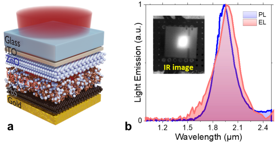
In this study, physicists have designed the first nanocrystal-based LED operating above 2 µm. To achieve this, a material that glows when electrically excited (HgTe) is sandwiched between a layer of zinc oxide (ZnO) and a layer of lead sulphide (PbS), these layers being in charge of the conduction of electrons and holes respectively. The device achieves an efficiency comparable to state-of-the-art LEDs in the same wavelength range (0.3% external quantum efficiency). A low activation voltage of 0.6 eV and an irradiance up to 3 W sr-1 m-2 are also achieved, which is already competitive in this spectral range. The operating mechanisms of the device, in particular the role of zinc oxide in tuning the charges and optimizing the efficiency, are consistently elucidated using three methods: electrical transport measurement, transient reflectivity spectroscopy, and time-resolved X-ray photoemission. Future work will focus on the performance of the device via improved tuning of the electrical potentials within the different layers and light extraction.
This work was conducted by the Paris Institute of Nanosciences (INSP, CNRS/Sorbonne University) in collaboration with 5 other French laboratories : Laboratoire d’optique appliquée (LOA, CNRS/ENSTA Paris/Ecole Polytechnique); Laboratoire de physique et d’étude des matériaux (LPEM, CNRS/ESPCI/Sorbonne Université); Centre de Nanosciences et de Nanotechnologies (C2N, CNRS/Université Paris-Saclay); Synchrotron SOLEIL; The French Aerospace Lab (ONERA). It has been published in Nature Photonics.